อ่าน 10 นาที
ลอจิกอาร์เรย์ที่ตั้งโปรแกรมได้
วงจรลอจิกอาร์เรย์ที่ตั้งโปรแกรมได้ ( PAL ) เป็นตระกูลของ เซมิคอนดักเตอร์ อุปกรณ์ลอจิกที่ตั้งโปรแกรมได้ ซึ่งใช้ในการสร้าง ฟังก์ชัน ลอจิก ใน วงจร ดิจิทัลซึ่งเปิดตัวโดย Monolithic...
ลอจิกอาร์เรย์ที่ตั้งโปรแกรมได้


วงจรลอจิกอาร์เรย์ที่ตั้งโปรแกรมได้ ( PAL ) เป็นตระกูลของ เซมิคอนดักเตอร์ อุปกรณ์ลอจิกที่ตั้งโปรแกรมได้ซึ่งใช้ในการสร้าง ฟังก์ชัน ลอจิก ใน วงจรดิจิทัลซึ่งเปิดตัวโดยMonolithic Memories , Inc. (MMI) ในเดือนมีนาคม พ.ศ. 2521 [ 1 ] MMI ได้รับเครื่องหมายการค้าจดทะเบียนในคำว่า PAL เพื่อใช้ใน "วงจรลอจิกเซมิคอนดักเตอร์ที่ตั้งโปรแกรมได้" ปัจจุบันเครื่องหมายการค้านี้เป็นของLattice Semiconductor [ 2 ]
อุปกรณ์ PAL ประกอบด้วย แกน PROM (หน่วยความจำอ่านอย่างเดียวที่ตั้งโปรแกรมได้) ขนาดเล็ก และวงจรลอจิกเอาต์พุตเพิ่มเติมที่ใช้ในการสร้างฟังก์ชันลอจิกที่ต้องการโดยใช้ส่วนประกอบเพียงไม่กี่ชิ้น
อุปกรณ์ PAL สามารถ "ตั้งโปรแกรมได้ในภาคสนาม" โดยใช้เครื่องมือเฉพาะทาง อุปกรณ์ PAL มีให้เลือกหลายแบบ:
- อุปกรณ์แบบ " ตั้งโปรแกรมได้ครั้งเดียว " (OTP) ไม่สามารถอัปเดตและนำกลับมาใช้ใหม่ได้หลังจากตั้งโปรแกรมครั้งแรกแล้ว (MMI ยังมีผลิตภัณฑ์ตระกูลเดียวกันที่เรียกว่า HAL หรือ "hard array logic" ซึ่งคล้ายกับอุปกรณ์ PAL ยกเว้นว่าได้รับการตั้งโปรแกรมแบบมาสก์จากโรงงานแล้ว)
- ชิปแบบลบได้ด้วยรังสียูวี (เช่น PALCxxxxx เช่น PALC22V10) มีหน้าต่างควอตซ์อยู่เหนือชิป และสามารถลบข้อมูลเพื่อนำกลับมาใช้ใหม่ได้โดยใช้แหล่งกำเนิดแสงยูวีเช่นเดียวกับEPROM
- รุ่นต่อมา (PALCExxx เช่น PALCE22V10) เป็นอุปกรณ์ที่สามารถลบข้อมูลได้ด้วยหน่วยความจำแฟลช
ในการใช้งานส่วนใหญ่ ปัจจุบัน GAL ที่ลบได้ด้วยไฟฟ้า ถูกนำมาใช้แทนPAL ที่ตั้งโปรแกรมได้ครั้งเดียวโดยตรง เนื่องจากขาเชื่อมต่อ เข้ากันได้
ประวัติศาสตร์
ก่อนที่จะมีการนำ PAL มาใช้ นักออกแบบวงจรลอจิกดิจิทัลจะใช้ ส่วนประกอบ แบบรวมขนาดเล็ก (SSI) เช่น ส่วนประกอบใน ตระกูล TTL ( transistor-transistor logic ) ซีรีส์ 7400ซึ่งประกอบด้วยบล็อกการสร้างลอจิกหลากหลายชนิด เช่น เกต ( NOT , NAND , NOR , AND , OR ), มัลติเพล็กเซอร์ (MUX) และดีมัลติเพล็กเซอร์ (DEMUX), ฟลิปฟลอป (D-type, JK เป็นต้น) และอื่นๆ อุปกรณ์ PAL หนึ่งตัวมักจะแทนที่แพ็คเกจลอจิกแบบ "แยกชิ้น" หลายสิบชิ้น ดังนั้นธุรกิจ SSI จึงลดลงในขณะที่ธุรกิจ PAL เติบโตขึ้น PAL ถูกนำไปใช้อย่างมีประสิทธิภาพในผลิตภัณฑ์หลายอย่าง เช่นมินิคอมพิวเตอร์ดังที่บันทึกไว้ในหนังสือขายดีของTracy Kidder เรื่องThe Soul of a New Machine
PALs were not the first commercial programmable logic devices; Signetics had been selling its field programmable logic array (FPLA) since 1975. These devices were completely unfamiliar to most circuit designers and were perceived to be too difficult to use. The FPLA had a relatively slow maximum operating speed (due to having both programmable-AND and programmable-OR arrays), was expensive, and had a poor reputation for testability. Another factor limiting the acceptance of the FPLA was the large package, a 600-mil (0.6", or 15.24 mm) wide 28-pin dual in-line package (DIP).
The project to create the PAL device was managed by John Birkner and the actual PAL circuit was designed by H. T. Chua.[3] In a previous job (at mini-computer manufacturer Computer Automation), Birkner had developed a 16-bit processor using 80 standard logic devices. His experience with standard logic led him to believe that user-programmable devices would be more attractive if the devices were designed to replace standard logic. This meant that the package sizes had to be more typical of the existing devices, and the speeds had to be improved. MMI intended PALs to be a relatively low cost (sub $3) part. However, the company initially had severe manufacturing yield problems and had to sell the devices for over $50. This threatened the viability of the PAL as a commercial product, and MMI was forced to license the product line to National Semiconductor. PALs were later "second sourced" by Texas Instruments and Advanced Micro Devices.
Process technologies
Early PALs were 20-pin DIP components fabricated in silicon using bipolar transistor technology with one-time programmable (OTP) titanium-tungsten programming fuses.[4] Later devices were manufactured by Cypress, Lattice Semiconductor and Advanced Micro Devices using CMOS technology.
The original 20- and 24-pin PALs were denoted by MMI as medium-scale integration (MSI) devices.
PAL architecture

The PAL architecture consists of two main components: a logic plane and output logic macrocells.
Programmable logic plane
The programmable logic plane is a programmable read-only memory (PROM) array that allows the signals present on the device pins, or the logical complements of those signals, to be routed to output logic macrocells.
PAL devices have arrays of transistor cells arranged in a "fixed-OR, programmable-AND" plane used to implement "sum-of-products" binary logic equations for each of the outputs in terms of the inputs and either synchronous or asynchronous feedback from the outputs.
Output logic
The early 20-pin PALs had 10 inputs and 8 outputs. The outputs were active low and could be registered or combinational. Members of the PAL family were available with various output structures called "output logic macrocells" or OLMCs. Prior to the introduction of the "V" (for "variable") series, the types of OLMCs available in each PAL were fixed at the time of manufacture. (The PAL16L8 had 8 combinational outputs, and the PAL16R8 had 8 registered outputs. The PAL16R6 had 6 registered and 2 combinational outputs, while the PAL16R4 had 4 of each.) Each output could have up to 8 product terms (effectively AND gates); however, the combinational outputs used one of the terms to control a bidirectional output buffer. There were other combinations that had fewer outputs with more product terms per output and were available with active high outputs ("H" series).[5]: 1–14 The "X" series of devices had an XOR gate before the register.[5]: 1–9 There were also similar 24-pin versions of these PALs.
This fixed output structure often frustrated designers attempting to optimize the utility of PAL devices because output structures of different types were often required by their applications. (For example, one could not get 5 registered outputs with 3 active high combinational outputs.) So, in June 1983 AMD introduced the 22V10, a 24-pin device with 10 output logic macrocells.[6] Each macrocell could be configured by the user to be combinational or registered, active high or active low. The number of product terms allocated to an output varied from 8 to 16. This one device could replace all of the 24-pin fixed function PAL devices. Members of the PAL "V" ("variable") series included the PAL16V8, PAL20V8 and PAL22V10.
 PAL 16R4 block diagram
 AMD 22V10 block diagram
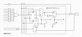 AMD 22V10 output macrocell


Programming PALs
PAL ถูกตั้งโปรแกรมด้วยระบบไฟฟ้าโดยใช้รูปแบบไบนารี (ในรูป แบบไฟล์ JEDEC ASCII / เลข ฐานสิบหก ) และระบบการตั้งโปรแกรมอิเล็กทรอนิกส์พิเศษที่มีให้จากผู้ผลิตหรือบุคคลที่สาม เช่นDATA I/Oนอกจากเครื่องตั้งโปรแกรมอุปกรณ์แบบหน่วยเดียวแล้ว ยังมักใช้เครื่องป้อนอุปกรณ์และเครื่องตั้งโปรแกรมแบบกลุ่มเมื่อต้องการตั้งโปรแกรม PAL มากกว่าสองสามตัว (สำหรับปริมาณมาก ต้นทุนการตั้งโปรแกรมด้วยระบบไฟฟ้าสามารถลดลงได้โดยให้ผู้ผลิตสร้างแม่พิมพ์โลหะแบบกำหนดเองเพื่อใช้ในการตั้งโปรแกรมรูปแบบของลูกค้าในขณะผลิต MMI ใช้คำว่า " hard array logic " (HAL) เพื่ออ้างถึงอุปกรณ์ที่ตั้งโปรแกรมด้วยวิธีนี้)
ภาษาโปรแกรม (เรียงตามลำดับการปรากฏตัว)

แม้ว่าวิศวกรบางคนจะตั้งโปรแกรมอุปกรณ์ PAL โดยการแก้ไขไฟล์ที่มีข้อมูลรูปแบบฟิวส์ไบนารีด้วยตนเอง แต่ส่วนใหญ่เลือกที่จะออกแบบตรรกะโดยใช้ภาษาอธิบายฮาร์ดแวร์ (HDL) เช่นABEL ของ Data I/O , CUPL ของ Logical Devices หรือPALASM ของ MMI โปรแกรม เหล่านี้เป็น โปรแกรม ช่วยออกแบบด้วยคอมพิวเตอร์ ( CAD ) (ปัจจุบันเรียกว่า " ระบบอัตโนมัติการออกแบบอิเล็กทรอนิกส์ ") ซึ่งแปล (หรือ "คอมไพล์") สมการตรรกะของผู้ออกแบบให้เป็นไฟล์แผนที่ฟิวส์ไบนารีที่ใช้ในการตั้งโปรแกรม (และมักจะทดสอบ) อุปกรณ์แต่ละตัว
ปาลาสม์
ภาษา PALASM ( มาจาก "PAL assembler") ได้รับการพัฒนาโดยJohn Birknerในช่วงต้นทศวรรษ 1980 และคอมไพเลอร์ PALASM ถูกเขียนโดย MMI ด้วยภาษา FORTRAN IV บนเครื่อง IBM 370/168 MMI ได้เผยแพร่ซอร์สโค้ดให้ผู้ใช้ใช้งานได้ฟรี ภายในปี 1983 ลูกค้าของ MMI ได้ใช้งานเวอร์ชันต่างๆ บนเครื่องDEC PDP-11 , Data General NOVA , Hewlett-Packard HP 2100 , MDS800และอื่นๆ
เดิมทีมีการใช้เพื่อแสดงสมการบูลีนสำหรับขาเอาต์พุตในไฟล์ข้อความ ซึ่งจะถูกแปลงเป็นไฟล์ 'แผนผังฟิวส์' สำหรับระบบการเขียนโปรแกรมโดยใช้โปรแกรมที่ผู้ผลิตจัดหาให้ ต่อมาตัวเลือกในการแปลงจากแผนผังวงจรก็เป็นที่นิยม และในเวลาต่อมา 'แผนผังฟิวส์' ก็สามารถ 'สังเคราะห์' ได้จากHDL (ภาษาอธิบายฮาร์ดแวร์ ) เช่นVerilog
คิวพีแอล
Assisted Technology released CUPL (Compiler for Universal Programmable Logic) in September 1983.[7] The software was always referred to as CUPL and never the expanded acronym. It was the first commercial design tool that supported multiple PLD families. The initial release was for the IBM PC and MS-DOS, but it was written in the C programming language so it could be ported to additional platforms.[8] Assisted Technology was acquired by Personal CAD Systems (P-CAD) in July 1985. In 1986, PCAD's schematic capture package could be used as a front end for CUPL.[9] CUPL was later acquired by Logical Devices and is now owned by Altium.[10] CUPL is currently available as an integrated development package for Microsoft Windows.[11]
Atmel releases for free WinCUPL (their own design software for all Atmel SPLDs and CPLDs). Atmel was acquired by Microchip in 2016.
ABEL
Data I/O Corporation released ABEL in April, 1984. The development team was Michael Holley, Mike Mraz, Gerrit Barrere, Walter Bright, Bjorn Freeman-Benson, Kyu Lee, David Pellerin, Mary Bailey, Daniel Burrier and Charles Olivier.
Data I/O spun off the ABEL product line into an electronic design automation company called Synario Design Systems and then sold Synario to MINC Inc in 1997. MINC was focused on developing FPGA development tools. The company closed its doors in 1998 and Xilinx acquired some of MINC's assets including the ABEL language and tool set. ABEL then became part of the Xilinx Webpack tool suite. Now Xilinx owns ABEL.
Device programmers
Popular device programmers included Data I/O Corporation's Model 60A Logic Programmer and Model 2900.
One of the first PAL programmers was the Structured Design SD20/24. They had the PALASM software built-in and only required a CRT terminal to enter the equations and view the fuse plots. After fusing, the outputs of the PAL could be verified if test vectors were entered in the source file.
Successors
After MMI succeeded with the 20-pin PAL parts introduced circa 1978, AMD introduced the 24-pin 22V10 PAL with additional features. After buying out MMI (circa 1987), AMD spun off a consolidated operation as Vantis, and that business was acquired by Lattice Semiconductor in 1999.[12]
Altera introduced the EP300 (first CMOS PAL) in 1983 and later moved into the FPGA business.
Lattice Semiconductor introduced the generic array logic (GAL) family in 1985, with functional equivalents of the "V" series PALs that used reprogrammable logic planes based on EEPROM (electrically eraseable programmable read-only memory) technology. National Semiconductor was a second source for GAL parts.

AMD introduced a similar family called PALCE. In general one GAL part is able to function as any of the similar family PAL devices. For example, the 16V8 GAL is able to replace the 16L8, 16H8, 16H6, 16H4, 16H2 and 16R8 PALs (and many others besides).
ICT (International CMOS Technology) introduced the PEEL 18CV8 in 1986. The 20-pin CMOS EEPROM part could be used in place of any of the registered-output bipolar PALs and used much less power.
Larger-scale programmable logic devices were introduced by Atmel, Lattice Semiconductor, and others. These devices extended the PAL architecture by including multiple logic planes and/or burying logic macrocells within the logic plane(s). The term complex programmable logic device (CPLD) was introduced to differentiate these devices from their PAL and GAL predecessors, which were then sometimes referred to as simple programmable logic devices (SPLDs).
Another large programmable logic device is the field-programmable gate array (FPGA). These are devices currently made by Intel (who acquired Altera) and Xilinx (who was acquired by AMD) and other semiconductor manufacturers.
See also
Further reading
- Books
- Programmable Logic Designer's Guide; Roger Alford; Sams Publishing; 1989; ISBN 0-672-22575-1. (archive)
- PAL Programmable Logic Handbook; 4ed; Monolithic Memories; 1985. (archive)
- Databooks
- เอกสารข้อมูล Bipolar LSI ปี 1984ฉบับที่ 5 บริษัทMonolithic Memoriesปี 1984 (เอกสารเก่า)
- ข้อกำหนด
- รูปแบบการถ่ายโอนข้อมูลมาตรฐานระหว่างระบบเตรียมข้อมูลและเครื่องโปรแกรมอุปกรณ์ลอจิกที่ตั้งโปรแกรมได้ ; มาตรฐาน JEDEC JESD3-C; JEDEC ; มิถุนายน 1994
สรุปเนื้อหา
ข้อมูลสำคัญจากบทความ
ข้อมูลสำคัญเกี่ยวกับ ลอจิกอาร์เรย์ที่ตั้งโปรแกรมได้
วงจรลอจิกอาร์เรย์ที่ตั้งโปรแกรมได้ ( PAL ) เป็นตระกูลของ เซมิคอนดักเตอร์ อุปกรณ์ลอจิกที่ตั้งโปรแกรมได้ ซึ่งใช้ในการสร้าง ฟังก์ชัน ลอจิก ใน วงจร ดิจิทัลซึ่งเปิดตัวโดย Monolithic...
ประวัติศาสตร์
ก่อนที่จะมีการนำ PAL มาใช้ นักออกแบบวงจรลอจิกดิจิทัลจะใช้ ส่วนประกอบ แบบรวมขนาดเล็ก (SSI) เช่น ส่วนประกอบใน ตระกูล TTL ( transistor-transistor logic ) ซีรีส์ 7400 ซึ่งประกอบด้วยบล็อกการสร้างลอจิกหลากหลายชนิด เช่น เกต ( NOT , NAND , NOR , AND , OR ),...
Process technologies
Early PALs were 20-pin DIP components fabricated in silicon using bipolar transistor technology with one-time programmable (OTP) titanium-tungsten programming fuses.
PAL architecture
The PAL architecture consists of two main components: a logic plane and output logic macrocells.